MATERIALS CHARACTERIZATION

Your proxy sample is not your device.

Thermal conductivity, interface resistance, and film properties measured on the actual multi-layer stack, not a bulk sample. NOSH-TDTR and POSH-TDTR give you the numbers your thermal model needs: spatially resolved, depth-profiled, and accurate across a wide range of advanced semiconductor materials.

THE MEASUREMENT GAP

Why thermal models fail at the material level

The inputs to your thermal simulation are only as good as the measurements they come from. For advanced semiconductor materials, those inputs are often wrong.

Bulk thermal conductivity values are not film values.

Handbook values for GaN, SiC, and diamond apply to bulk crystals. Thin-film and epitaxial layers have dramatically different thermal conductivity due to phonon boundary scattering and impurities. Your simulation is using the wrong number.

Interface resistance is the dominant thermal bottleneck.

In GaN-on-SiC and GaN-on-diamond packages, the thermal boundary resistance at the growth interface, not the bulk thermal conductivity, limits heat extraction. This value cannot be looked up. It must be measured on your specific material stack.

In-plane ≠ cross-plane

Many advanced semiconductor materials and interfaces are thermally anisotropic. Cross-plane conductivity (relevant for heat extraction through the substrate) can differ from in-plane conductivity (relevant for lateral heat spreading) by an order of magnitude or more.

Process variation changes thermal properties.

Growth conditions, doping levels, and process steps all affect thermal conductivity and interface resistance. A material characterized at the wafer center may differ from the wafer edge by 20–30%. Simulation inputs must reflect your specific process.

OUR TECHNIQUES

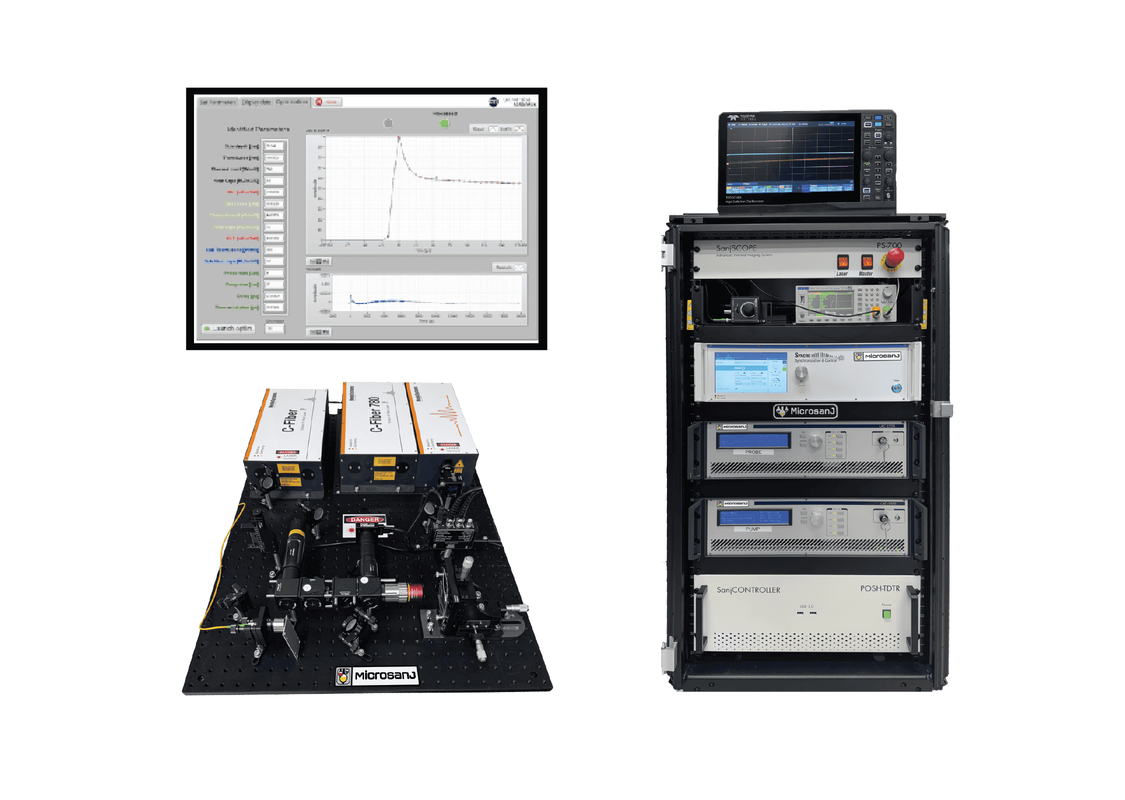
Two Techniques, One Platform – NOSH-TDTR and POSH-TDTR

Microsanj’s SANJ Platform offers both nanosecond and picosecond TDTR on commercial systems. Understanding which technique to use depends on the measurement goal, the material stack, and the film thickness range.

NEW

NOSH-TDTR™ (Add-on EZ530 / NT220)

Nanosecond optical sampling. Full-field thermoreflectance with pump-probe capability. Measures in-plane thermal conductivity with sub-micron spatial resolution. Can be performed on the same setup as device thermal imaging, enabling materials characterization and device imaging without moving the sample.

NEW

POSH-TDTR™ (PS700 system)

Picosecond optical sampling. Femtosecond laser pump + probe at 50 MHz. The gold-standard TDTR technique, superior to FDTR and SSTR for cross-plane characterization. Measures both in-plane and cross-plane thermal conductivity, thermal boundary resistance, and film thickness from ~10 nm to several microns. SanjTHERM™ AI parameter extraction eliminates time-consuming FEA.

Capability NOSH-TDTR™ POSH-TDTR™
In-plane thermal conductivity ✓ ✓
Cross-plane thermal conductivity Partial ✓Best-in-class
Thermal boundary resistance (TBR) ✓ ✓
Full-field spatial mapping ✓Sub-micron —Point measurement
Film thickness measurement — ✓~10 nm to µm
Anisotropic materials — ✓
Add-on to existing system ✓EZ530 / NT220 Standalone PS700
Standalone system required — ✓PS700
Acquisition speed Nanosecond 5 ps / <5 ms per sweep
AI parameter extraction (SanjTHERM™) ✓ ✓
Works alongside device thermal imaging ✓Same setup —Separate system

0.1–1000 W/m·K

Conductivity range consistent over 10³

10 nm

Minimum film thickness
POSH-TDTR

±1°C

Repeatability ~10% accuracy

<5 ms

Per sweep acquisition parameter extraction: minutes

MATERIALS COVERAGE

Every material in your device stack

Microsanj systems are calibrated and validated for the full range of advanced semiconductor materials from sub-1 W/m·K polymers to 2000+ W/m·K diamond.

Semiconductor Substrates Thin Films & Interfaces Advanced Packaging Structures
GaN / GaN-on-SiC / GaN-on-SiTBR at growth interface, epitaxial layer conductivity, buffer layer properties Metal films (Cu, Au, Pt, Al)Film thickness, grain-boundary-limited conductivity Through-silicon vias (TSVs)Cu fill conductivity, TSV-to-substrate interface resistance, voiding detection
SiC (4H-SiC, 6H-SiC)Substrate thermal conductivity, anisotropic in-plane vs. cross-plane Dielectrics (SiO₂, Al₂O₃, HfO₂)Gate oxide TBR, inter-layer dielectric conductivity Bonded wafer interfacesHybrid bonding, direct bonding, and fusion bonding TBR
Diamond / GaN-on-DiamondTBR at GaN-diamond interface — the critical bottleneck for GaN-on-diamond devices Thermal interface materials (TIMs)Bond-line thickness, effective conductivity under compression Si interposers / RDLRedistribution layer thermal properties, interposer conductivity
Ga₂O₃ / AlGaN / InGaNUltra-wide-bandgap materials; low thermal conductivity characterization Polymers/epoxiesDie-attach materials, underfill, encapsulant thermal properties Embedded RF modules (AoC/AiP)Antenna-in-package substrate thermal characterization
FREE WEBINAR

Nanosecond & Picosecond Pump-Probe Techniques For Thermal Characterization of Advanced Packages

Nanosecond and picosecond thermoreflectance imaging applied to real 3DHI structures, buried interfaces, cross-plane conductivity, and phase-delay depth analysis on operating devices. Featuring Prof. Ali Shakouri (Purdue / Microsanj), Dr. Stefan Dilhaire (University of Bordeaux), and Prof. Srabanti Chowdury (Stanford)

Two measurement modes: full-field megapixel lock-in thermoreflectance for die-level hot spot detection in 3D stacked structures, plus single-point transient analysis for extracting in-plane and cross-plane thermal conductivity in bulk, thin-film, and multilayer materials — all built on a pump-probe TDTR framework spanning nanosecond and picosecond optical sampling regimes.

Application areas: wide bandgap device characterization (GaN, SiC, and related materials) and industry failure analysis/reliability workflows where optical sampling replaces destructive physical analysis.

Getting started: deployment options, upgrade paths, and testing services.

FAQ

Common questions from materials engineers

What is the difference between NOSH-TDTR and POSH-TDTR?

NOSH-TDTR (Nanosecond Optical Sampling) uses a nanosecond pump laser and measures primarily in-plane thermal conductivity with sub-micron spatial resolution. It can be performed as a full-field imaging mode alongside device thermal imaging on the same system. POSH-TDTR (Picosecond Optical Sampling) uses a femtosecond laser at 50 MHz repetition rate and provides the highest accuracy for cross-plane thermal conductivity, thermal boundary resistance, and film thickness. POSH-TDTR is the technique of choice when cross-plane properties or sub-10 nm film characterization are required. NOSH-TDTR is preferred when spatial mapping with sub-micron resolution is the priority.

How does POSH-TDTR compare to FDTR and SSTR?

All three are pump-probe laser techniques for thermal property measurement. FDTR (Frequency-Domain Thermoreflectance) modulates the pump at variable frequency and measures phase response, good for in-plane conductivity but less sensitive to cross-plane properties and TBR in thin-film stacks. SSTR (Steady-State Thermoreflectance) measures steady-state temperature and is well-suited for thick substrates. POSH-TDTR operates in the time domain with picosecond resolution, which gives it the highest sensitivity to interfaces and thin films, particularly important for the GaN-on-SiC and GaN-on-diamond stacks relevant to power and RF devices. Microsanj's POSH-TDTR also includes SanjTHERM™ AI-assisted parameter extraction, which eliminates the need for manual FEA fitting and significantly reduces analysis time.

What sample preparation is required?

Both NOSH-TDTR and POSH-TDTR are non-destructive and require minimal sample preparation. For standard measurements, a thin metal transducer layer (typically 80–100 nm of Al or Pt) is deposited on the sample surface by sputtering or evaporation. The transducer absorbs the pump pulse and converts it to a thermal signal. For samples where a transducer cannot be deposited, for example, if the surface is already metallized or if the measurement must be truly non-contact, alternative measurement configurations are available. Contact the team to discuss your specific sample structure.

Can NOSH-TDTR and device thermal imaging be performed on the same sample without moving it?

Yes. NOSH-TDTR is available as an add-on to the SanjSCOPE EZ530 and NT220 systems. Because both capabilities operate on the same optical platform, a device can be characterized for thermal properties (conductivity, TBR) and then immediately imaged under operating bias for device-level thermography without removing the sample from the probe station or changing the optical setup. This is particularly powerful for correlating material properties at a specific location with the device's thermal behavior at that same location.

Ready to measure the actual material in your stack?

Send us your substrate, film, or device sample, and we'll run NOSH-TDTR or POSH-TDTR at our global laboratories and deliver a full materials characterization report. No commitment necessary.