Metals are invisible to IR cameras
Gold bond pads, aluminum contacts, and copper heatsink surfaces have near-zero emissivity. IR imaging produces noise, not temperature data, on any metal surface.

Metal contacts have near-zero emissivity. Photonic waveguides are too small for IR. Pulsed lasers blind conventional imagers. Thermoreflectance imaging solves all three.


435 nm
500 ps
<1 mK
30%
Three fundamental physics problems make conventional IR cameras unreliable for photonic device characterization. Thermoreflectance imaging solves each one.
Gold bond pads, aluminum contacts, and copper heatsink surfaces have near-zero emissivity. IR imaging produces noise, not temperature data, on any metal surface.
LWIR cameras resolve ~30 µm per pixel. Silicon photonic waveguides are 7–10 µm wide. A localized hot spot at the waveguide input is physically invisible to IR at any magnification.
GaAs lasers at 808 nm and InP lasers at 1310/1550 nm: the device's own optical output floods any co-located imager. A filter and gated illumination scheme are required to separate the thermal signal from the laser output.
Limitation — conventional IR
Advantage — thermoreflectance
Characterization results across every major photonic device class, all using Microsanj thermoreflectance systems.
III-V Laser Diode
Transient thermal response at 100x magnification, resolving two distinct material regions (InP substrate vs. InP-modified material) under a 250 mA pulse. Time range 1 µs to 100 µs captured in a single acquisition.
High-Power Laser Bar
Surface temperatures of the GaAs laser facet and the CuW heatsink are measured simultaneously. Requires a filter to block the 808 nm laser output during TR imaging. Both topside and front-facet imaging configurations supported.
Silicon Photonics — Detector
3D heat distribution mapped along a 250 µm waveguide with a 7.4 µm channel width. Peak surface temperature exceeds 200°C at the waveguide input. Results validated quantitatively against a COMSOL finite-element simulation.
High-Power Photodetector
Thermal impedance measured at 520 K/W, 1.7× lower than a comparable InP/InGaAs device using thermoreflectance to verify the COMSOL simulations; substrate-induced heating distinguished from junction heating.
High-Linearity Photodetector
Surface temperature mapped on 34 µm and 40 µm diameter mesa devices under varying heat generation levels. Thermal runaway onset was identified and compared against an ANSYS simulation for packaging design optimization.
Die Attach — Package Thermal
Passivation layer comparison for semiconductor laser bars mounted on silicon substrates: poly-silicon reduces thermal resistance by ~30% vs. silicon dioxide. Solder voids and thermal islands in the copper heatsink were identified non-invasively.
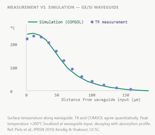
Analytical and finite-element thermal models for photonic devices make assumptions about heat source distribution, thermal conductivity, and boundary conditions that are difficult to verify from first principles alone.
Thermoreflectance imaging provides a direct, spatially resolved surface temperature measurement to validate or refine COMSOL, ANSYS, and Beamprop models before a design is committed to fabrication.
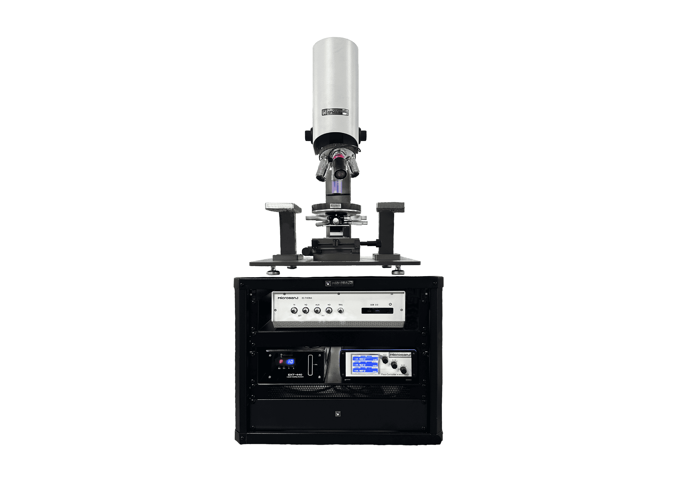
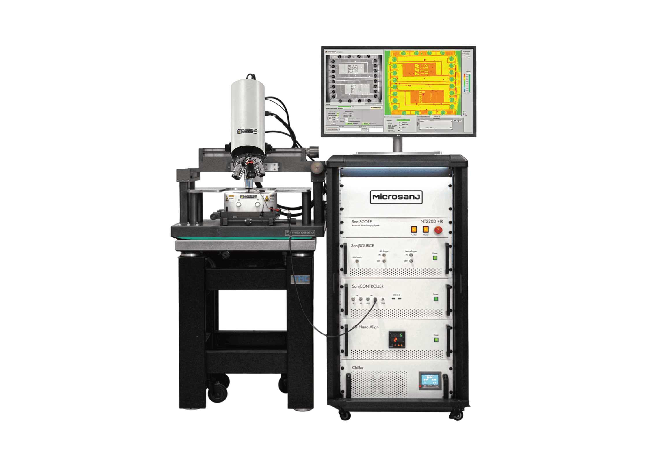
The SanjSCOPE™ EZ-THERM and NT220 series support every photonic characterization scenario, with software-selectable wavelengths and interchangeable objectives.
Our applications team has hands-on experience with laser, photodetector, and silicon photonics characterization. Tell us your device and measurement goals.