






RF, 5G & 6G DEVICE ANALYSIS

Your DC I-V curve is incomplete.

GaN HEMTs, SiC power transistors, and mmWave amplifiers fail in ways that DC characterization and IR thermography simply cannot explain. Thermoreflectance imaging combined with pulsed-IV correlation reveals what's actually happening in nanoseconds, at sub-micron resolution, on the device under real operating conditions.

Trusted by

THE MEASUREMENT GAP

Why RF Device characterization fails at the domain boundary

Every RF device engineer has encountered this: models that predict one thing, devices that do another. The gap is almost always a thermal measurement problem.

IR thermography reports the wrong temperature

SiC and other wide band-gap materials are largely transparent in the IR band you're measuring substrate emission, not the channel. The 2DEG where heat concentrates is sub-micron and invisible to IR's diffraction limit. Your thermal resistance is wrong before the model starts.


DC I-V conflates self-heating with trap effects

DC characterization runs at thermal equilibrium not the condition that matters for RF operation. Self-heating and trap dynamics produce the same signature in DC data. Pulsed-IV at sub-microsecond timescales is the only way to separate them.

Standard thermal tools are too slow for RF switching

GaN and SiC devices operate at switching timescales from nanoseconds to microseconds. Lock-in based IR systems resolve thermal events at 10 µs, three to four orders of magnitude too slow to see what's happening during a switching transient.

Disconnected measurement domains produce disconnected models

RF, electrical, and thermal characterization are run on separate equipment, at different times, in different labs. The correlation between what the electrical model predicts and what the device thermally experiences is never verified. The model is complete and wrong.

THE SOLUTION

Correlated thermoreflectance + pulsed-IV on the same device

Microsanj systems synchronize full-field thermoreflectance imaging with your RF and pulsed-IV measurements on the same device, at the same bias point, without moving the probe. The result is a complete, correlated picture of electrothermal behavior that no single-domain measurement can produce.

1 Apply pulsed-IV bias

Sub-microsecond pulses isolate intrinsic device behavior from self-heating. Current collapse, knee walkout, and threshold-voltage dispersion become visible as distinct signatures, not conflated noise.

2 Synchronized thermal acquisition

Thermoreflectance imaging triggers from the same electrical stimulus. The thermal map is captured at a specific timepoint — 50 ns or 500 ps — synchronized to the pulsed bias. The image shows thermal state at that precise moment.

3 Full-field, sub-micron thermal map

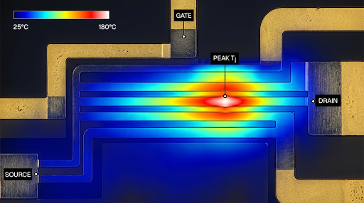
The entire device is imaged simultaneously at sub-300 nm resolution. Gate hotspots, source-drain asymmetry, current crowding, and interface heating are all visible. Defect localization takes seconds, not days.

4 Electrothermal model validation

Real thermal maps provide ground truth for your electrothermal model at every bias point. Model error is identified and corrected before it propagates into PA design and reliability prediction.

<250 nm

Spatial resolution at 50x

50 ns

Standard temporal resolution NT220 Series 

500 ps

Optional upgrade captures RF switching transients

±0.1°C

Temperature resolution CTR calibration ±0.5×10⁻⁵

CAPABILITIES

What Microsanj reveals in RF devices

The SANJ Platform addresses specific measurement failure modes in GaN, SiC, and mmWave device characterization.

Gate Hotspot Localization

Sub-micron resolution resolves the 2DEG temperature at the gate edge, the actual failure location, not the device average. Reveals gate-to-gate non-uniformity across multi-finger HEMTs.

Trap effect separation

Pulsed-IV + thermoreflectance correlation at multiple quiescent bias points separates self-heating from gate and buffer-trap effects. Maps trapping dynamics to specific device regions.

RF switching transient capture

500 ps temporal resolution captures thermal events at RF operating timescales, switching transients, pulsed operation, and self-heating dynamics that 10 µs lock-in systems cannot see.

Wafer-level thermal mapping

Automated probe station integration (MPI TS3500) enables full-wafer thermal characterization scripted, unattended, die-by-die. Identifies thermal outliers that pass the electrical test but show early-failure signatures.

Electrothermal model validation

Full-field thermal maps at calibrated bias points provide ground truth for electrothermal simulation. Spatial temperature distribution, thermal resistance, and self-heating dynamics are all measurable.

Failure analysis at the probe station

When a device fails electrically at the probe station, thermoreflectance imaging captures the thermal map immediately on-wafer, without de-probing or shipping. Root cause in minutes, not days.

FREE WEBINAR

Multiphysics Characterization of GaN and Wide-Bandgap RF Devices

Featuring leading experts from the Colorado School of Mines, the University of Maryland, Purdue University, and MPI Corporation you’ll learn how thermoreflectance uncovers a deeper understanding of GaN, SiC, and next-generation semiconductors.

Electrothermal coupling is real – RF gain, noise figure, and reliability all degrade with temperature — but the coupling is nonlinear and hot spots play a key role. Measuring thermally without an RF context leaves critical information on the table.

Pulse IV reveals what DC hides – pulsed measurements isolate the intrinsic device behavior from self-heating and trap effect, giving a cleaner picture of what's really limiting performance.

Thermal imaging closes the loop – Full-field thermoreflectance imaging maps where the heat actually goes, validating models, identifying hotspots, and connecting device behavior to reliability outcomes.

The only commercial system that resolved our GaN channel hotspots at the spatial resolution we needed for PA reliability validation. IR didn’t even come close.

RF Device Engineer

Defense Electronics, US

Pulsed-IV correlated with thermoreflectance gave us a completely different picture of trap behavior versus self-heating. Our SPICE model accuracy improved significantly.

Research Engineer

RF Power Device Group

Before, we were modeling thermal behavior based on static assumptions. Seeing the electrothermal coupling in real-time, at the sub-microsecond scale, has fundamentally validated our multiphysics research.

Principal Investigator

Semiconductor Research Lab

FAQ

Common questions from RF design engineers

Why does IR thermography underreport GaN-on-SiC temperature?

SiC is largely transparent in the mid-infrared band. When you image a GaN-on-SiC device with an IR camera, the signal you capture includes significant emission from the SiC substrate, not just the GaN channel, where heat actually concentrates. The 2DEG at the gate, the actual hotspot location is sub-micron and below IR's diffraction limit. The result is systematic underestimation of channel temperature, often by a factor of 2× or more. Thermoreflectance imaging uses visible and near-UV light, which reflects from the GaN surface directly. The substrate transparency issue does not apply.

What temporal resolution do I need for GaN RF characterization?

It depends on what you're measuring. For most thermal resistance and steady-state characterization, the NT220-Series 50 ns resolution is sufficient. For capturing switching transients in pulsed PA operation, 5G envelope signals, or pulsed radar waveforms, the 500 ps upgrade is required. The 500 ps option is also necessary if you're separating self-heating from trap effects at short bias pulse widths; anything shorter than ~10 ns requires picosecond-class temporal resolution to capture the thermal response before traps have time to respond.

Can I use my existing probe station with Microsanj systems?

Yes. Microsanj systems are designed to integrate with many existing probe stations. The strategic partnership with MPI Corporation provides a turnkey integration with the MPI TS3500 for automated wafer-level characterization. For other probe station platforms, the Microsanj optical head mounts to a standard microscope port and can be configured for your existing setup. Contact us to discuss your specific probe station configuration.

How does thermoreflectance imaging work on GaN devices specifically?

The fundamental equation is ΔR/R = C_TR · ΔT, where the thermoreflectance coefficient C_TR is material and wavelength-dependent. For GaN, illumination at 365 nm provides a strong thermoreflectance coefficient and spatial resolution of 281 nm, resolving individual gate fingers in a standard GaN HEMT. The system calibrates C_TR for each material, and temperature change is extracted per pixel from the measured reflectance change. The full CCD array captures all pixels simultaneously, so the entire device is imaged in a single acquisition.

What’s the difference between NOSH-TDTR and a standard thermoreflectance measurement?

Standard thermoreflectance imaging measures the surface temperature of an operating device. It's a full-field measurement of ΔT across the device at a specific moment in time. NOSH-TDTR (Nanosecond Optical Sampling TDTR) is a materials characterization add-on that uses a nanosecond pump-probe technique to extract thermal properties, thermal conductivity, thermal boundary resistance, and film thickness from the material stack. Both measurements can be performed on the same system. NOSH-TDTR is particularly valuable for characterizing the GaN-on-SiC or GaN-on-diamond interface thermal resistance that determines how efficiently heat leaves the device.

Ready to see inside your RF devices?

Send us a GaN or SiC device and we'll run a complimentary thermoreflectance measurement at one of our global laboratories. No obligation.