












ADVANCED PACKAGING & 3DHI

Heat doesn't move the way your model says it does.

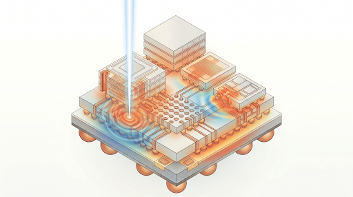
3D heterogeneous integration stacks materials with radically different thermal properties, GaN, SiC, Cu, diamond, polymers, and dielectrics in a single package. Thermal failures form at buried interfaces that your surface measurement cannot reach. Microsanj sees inside.

Trusted by

THE 3DHI THERMAL CHALLENGE

Why 3D packaging creates thermal measurement problems that 2D tools can't solve

Every advance in packaging density creates a new thermal measurement problem. Surface thermometry gives you the exit temperature, not the source.

Buried interfaces are where failures actually occur.

Thermal boundary resistance at bonded interfaces, hybrid bonding layers, and die-attach materials determines heat flow through the package. These interfaces are inaccessible to surface thermometry. You see the effect on the surface, not the cause buried inside.
Cross-plane ≠ in-plane at every layer

Stacked dies, interposers, and RDL layers all have different in-plane and cross-plane thermal conductivities. Heat spreading behavior is fundamentally 3D in a 3DHI package. A 2D surface measurement of any kind gives you an incomplete and potentially misleading picture.

IR thermography can't see below the top surface.

In a 3DHI package, the chip generating heat may be the third die down. IR imaging shows the surface temperature of whatever is on top. The thermal path from the source to the exit, through multiple layers each with its own conductivity and interface resistance, is invisible to surface measurements.

Simulation inputs don't account for process variation.

Thermal simulations use handbook values for material conductivity and assume ideal interfaces. Real TBR values depend on growth conditions, surface preparation, and bonding process. The model is only as accurate as the measured inputs it receives.

HOW MICROSANJ ADDRESSES 3DHI

Three measurement capabilities for a complete 3DHI thermal picture

No single measurement technique covers the full range of what 3DHI packages require. Microsanj provides a platform that combines die-level thermal imaging, depth-resolved materials characterization, and interface resistance measurement on the same system.

1 Full-field thermal imaging of operating dies

Thermoreflectance imaging captures the temperature distribution across every operating die simultaneously at sub-micron spatial resolution. Hotspot location, die-to-die thermal coupling, and power distribution are all visible in a single acquisition.

2 Thermal boundary resistance at bonding interfaces

NOSH-TDTR and POSH-TDTR measure interface thermal resistance directly at hybrid bonding layers, die-attach interfaces, and Cu-Cu bonding structures. The measured TBR value for your specific bonding process is not a handbook estimate.

3 Depth-resolved phase analysis

Phase-delay analysis of the pump-probe signal encodes depth information because different layers respond to different thermal diffusion timescales. The depth of a thermal anomaly can be extracted from the phase shift, enabling 3D localization without cross-sectioning.

4 SanjTHERM™ model validation

Measured thermal properties (conductivity, TBR, film thickness) feed directly into SanjTHERM™ for thermal model parameter extraction and validation. The model is grounded in your measured material stack, not assumed values.

<250 nm

Spatial resolution for die-level thermal imaging

10 nm–cm

Depth range surface to substrate

Non-destructive

No cross-sectioning required package remains intact

0.1–1000 W/m·K

From polymers to diamond

OUR SYSTEMS

Two SanjSCOPE™ systems, one configurable platform

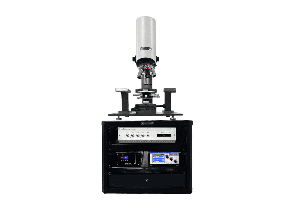
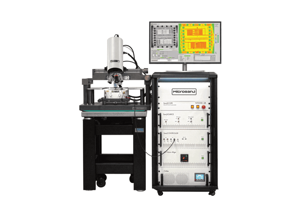
The SanjSCOPE™ EZ-THERM EZ530 and NT220-Series deliver dual-mode thermoreflectance and IR imaging for active device R&D and production, differing in transient resolution from microseconds down to picoseconds. Both support the NOSH-TDTR add-on, so you can start with the system your application needs today and extend its capability as your measurement requirements grow.

NEW

SanjSCOPE™ EZ-THERM EZ530

Active device R&D and production. Dual mode Thermoreflectance + IR. Up to 3 sensors.

  • 50 µs / 5 µs transient
  • NOSH-TDTR add-on
NEW

SanjSCOPE™ NT220-Series

Active device R&D and production. Dual mode Thermoreflectance + IR. Up to 3 sensors.

  • 50 ns / 500 ps transient
  • NOSH-TDTR add-on
USE CASES

Where Microsanj makes the difference in 3DHI

Hybrid bonding TBR measurement

Measure thermal boundary resistance at Cu-Cu hybrid bonding interfaces. Validate that the bonding process achieves design-intent thermal performance before packaging.

Buried hotspot localization

Phase-delay analysis identifies the depth of a thermal anomaly without cross-sectioning. Localize a hotspot to a specific layer in a stacked structure non-destructively.

TSV integrity characterization

Through-silicon via thermal conductivity and interface resistance detect voids, delamination, and fill quality defects through thermal property measurement rather than destructive analysis.

Die-attach material qualification

Characterize TIM conductivity, bond-line thickness, and interface resistance for die-attach materials under real operating conditions. Compare candidate materials quantitatively.

Wafer-level thermal uniformity

Automated wafer-level thermal mapping with MPI probe station integration. Identify process variation in thermal properties across a wafer before dicing and packaging.

Thermal simulation validation

Provide measured material inputs (conductivity, TBR) to replace assumed handbook values in your thermal model. Ground your simulation in your actual process, not textbook values.

FREEE WEBINAR

Nanosecond & Picosecond Pump-Probe Techniques For Thermal Characterization of Advanced Packages

Nanosecond and picosecond thermoreflectance imaging applied to real 3DHI structures, buried interfaces, cross-plane conductivity, and phase-delay depth analysis on operating devices. Featuring Prof. Ali Shakouri (Purdue / Microsanj), Dr. Stefan Dilhaire (University of Bordeaux), and Prof. Srabanti Chowdury (Stanford)

Two measurement modes: full-field megapixel lock-in thermoreflectance for die-level hot spot detection in 3D stacked structures, plus single-point transient analysis for extracting in-plane and cross-plane thermal conductivity in bulk, thin-film, and multilayer materials — all built on a pump-probe TDTR framework spanning nanosecond and picosecond optical sampling regimes.

Application areas: wide bandgap device characterization (GaN, SiC, and related materials) and industry failure analysis/reliability workflows where optical sampling replaces destructive physical analysis.

Getting started: deployment options, upgrade paths, and testing services.

COMMUNITY VALIDATED

Used across the advanced packaging research and production ecosystem


Measured TBR replaced a handbook assumption

A 3DHI packaging team running thermal simulation on a hybrid bonded stack found their assumed interface resistance was 3× lower than the measured value from POSH-TDTR. Correcting that single input brought the simulation error from ~35% down to under 9% without changing anything else in the model.

Root cause found without cross-sectioning

A reliability team investigating intermittent thermal failures in a stacked die package used phase-delay TDTR to localize the anomaly to a specific bonding layer non-destructively, on an intact package. The defect was confirmed and the process corrected before a single wafer was cross-sectioned.

Process variation that the electrical test missed

A wafer-level thermal mapping run across a 200 mm wafer revealed a 28% variation in die-attach thermal resistance from center to edge. Every die passed the electrical test. The thermal outliers were identified and removed before packaging, avoiding field failures downstream.

FAQ

Common questions from packaging engineers

Can Microsanj measure thermal properties inside a fully packaged 3DHI structure?

Partially. Thermoreflectance imaging and NOSH-TDTR work from the top surface, so they directly access whatever is the exposed die surface, interposer, or package lid if optically transparent. For buried interface characterization, POSH-TDTR uses phase-delay analysis to extract depth information without physical access to the interface. A thin metal transducer on the top surface is still required to absorb the pump pulse. For structures where there is no optical access at all, the testing services team can discuss the best approach for your specific package architecture.

What thermal boundary resistance values are typical for hybrid bonding?

TBR at Cu-Cu hybrid bonding interfaces varies significantly with surface preparation, anneal conditions, and bonding process. Published research reports values ranging from roughly 1 to 50 MW/m²·K, a 50× range that makes handbook assumptions unreliable. The value for your specific process is the only number that matters for your thermal simulation, and it must be measured. POSH-TDTR on a process control monitor (PCM) structure can provide this measurement with ±10% accuracy.

How is this different from what we'd get from thermal simulation alone?

Thermal simulation predicts what should happen given the material properties you input. If those inputs are wrong and for advanced packaging materials, they usually are the simulation output is usually wrong. Microsanj measurement provides the ground truth: the actual thermal conductivity and TBR of your specific material stack under real conditions. The two tools are complementary, not competing: measurement provides the accurate inputs that make simulation predictive rather than approximate.

Is the testing service appropriate for pre-production samples?

Yes, the testing service is specifically designed for customers who want to validate measurement capability before committing to a system purchase. Pre-production, engineering samples, and research wafers are all suitable. An NDA can be executed before samples are submitted. The testing team will provide a measurement report, and the testing cost is credited toward a system purchase if you decide to proceed. Typical turnaround is 2–3 weeks, depending on sample complexity.

See inside your 3DHI package

Send us a sample wafer, package, or die. We'll show you the thermal boundary resistance, buried hotspot, or material property you've been trying to measure. No commitment required.