See Inside. Measure Everything: Introducing the Next Era of Microsanj
For nearly two decades we built under one banner, The Future of Thermal Imaging. Today, we’re retiring it. Microsanj is now a complete platform for Advanced Semiconductor, Optical, and Thermal Characterization.


In 2007, Microsanj pioneered high-resolution thermoreflectance to give semiconductor engineers a level of visibility that traditional infrared cameras simply could not reach, precise mapping of sub-micron hotspots inside active devices.
But the landscape has changed. With the rise of heterogeneous integration (3DHI), wide-bandgap materials like GaN and SiC, ultra-dense RF microelectronics, and silicon photonics, heat is no longer a simple structural byproduct. It’s a complex, multi-physics bottleneck buried deep within advanced packaging and atomic-scale material interfaces.
Our technology advanced alongside those challenges. So we’re stepping into a new chapter, with a new category and a new motto: See Inside. Measure Everything. Microsanj is no longer just a thermal imaging company.
Our customers are no longer just dealing with localized hotspots on a bulk substrate; they are managing complex dynamic electrothermal pathways across atomic interfaces and 3D heterogeneous packaging. Moving from ‘The Future of Thermal Imaging’ to ‘See Inside. Measure Everything.’ reflects our evolution from an advanced imaging utility to an indispensable multi-domain characterization platform.
 Dr. Mo ShakouriCEO, Microsanj
Three domains. One configurable platform.
The revamped SanjSCOPE™ family breaks down the silos between standalone test environments. Microsanj is now the only commercial provider that bridges thermal imaging, materials characterization, and multiphysics RF/EM field imaging on a single, upgradable architecture.
DOMAIN 01
Advanced active device thermal imaging
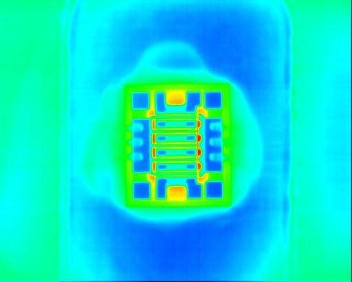
Our core, industry-standard technology, supercharged. Pairing full-field CCD-based thermoreflectance (TR) with macro-scale IR gives engineers a dual-mode system that instantly locates a macro hotspot, then zooms to sub-micron features.
- Unparalleled resolution: sub-300 nm spatial resolution, with temporal resolution from 50 µs down to 500 ps to capture real-time RF switching dynamics.
- Piezo auto-calibration: eliminates time-consuming manual calibration, delivering absolute temperature measurements down to ±0.1°C.

DOMAIN 02
Nanosecond & picosecond materials characterization (TDTR)
Through our proprietary NOSH-TDTR™ and standalone POSH-TDTR™ systems, we’ve commercialized the gold standard of optical sampling and brought it straight to the active device validation lab.
- Real device analysis: measure in-plane and cross-plane thermal conductivity (<1 to 1000 W/m·K) and Thermal Boundary Resistance (TBR) directly on your actual device stack, not an isolated proxy sample.
- Instant parameter extraction: SanjTHERM™ software extracts thin-film thermal data in minutes, bypassing tedious manual finite element analysis (FEA).

For years, measuring interface thermal resistance and ultra-thin film conductivity required dedicated academic setups and non-standard sample prep. Microsanj’s commercial integration of TDTR onto actual device topographies is a major practical milestone for engineers struggling to validate sub-surface material boundaries under real thermal stress.
 Dr. David CahillGrainger Distinguished Chair in Engineering
DOMAIN 03
Multiphysics and RF/EM field imaging
Devices don’t operate in a thermal silo, temperature, electrical behavior, and electromagnetic fields are deeply interconnected.
- Electrothermal correlation: by synchronizing pulsed-IV measurements with fast thermoreflectance imaging, the platform separates active self-heating from trap effects in GaN HEMTs, proving what static DC I-V curves hide.
- Integrated S-parameter, pulsed-IV, and thermal analysis: through strategic integration with probe-station leaders like MPI, engineers get a fully synchronized multiphysics workflow, a simultaneous view of electrical performance and thermal response, with immediate failure localization on-wafer and no need to de-probe or ship samples to external labs.

The integration of Microsanj’s thermal imaging capabilities with MPI’s state-of-the-art probe stations effectively bridges the gap between electrical test and thermal validation, allowing customers to choose between fully automated scripting or optimized probe access, all without needing to de-probe the wafer, thereby accelerating client time-to-market.
 Vince MalletteDirector of Global Sales & Marketing, MPI Corporation
As wide-bandgap electronics push into higher power densities and mmWave frequencies, measuring the thermal response of the electronics is critical, but only half the battle. You have to understand how the localized thermal field is driven by the current and the electric field distribution, as well as the pathways through which heat dissipates from the device. All of these factors affect thermal management and reliability during actual device operation. This holistic platform approach provides solutions for multiphysics validation of device models and device designs that wide-bandgap and 3DHI workflows need to be successful.
 Dr. Sam GrahamDean of Engineering, University of Maryland
Built for the way infrastructure is actually wired
Semiconductor labs can’t simply rip out and replace their capital infrastructure, so the SanjSCOPE™ platform is engineered to extend your existing investments, not replace them.
Through our automation partnership with MPI Corporation, our optical heads integrate seamlessly onto automated wafer probe stations like the MPI TS3500. That enables full, scripted wafer-level thermal mapping: run an electrical test, detect a failure, and trigger an immediate in-situ thermal map, without ever removing the sample.

To successfully debug tomorrow’s advanced architectures, engineers need a tight, real-time loop between physical measurements and digital twin predictive models. Single-domain tracking is an engineering blind spot. By integrating optical thermography, transient materials analytics, and near-field EM profiling into one physical environment, we eliminate the guesswork from multi-physics analysis.
 Dr. Ali ShakouriCTO, Microsanj
See inside your own device
Ready to see what you’ve been missing?
Whether you’re validating wide-bandgap PA reliability, debugging 3D heterogeneous packaging bottlenecks, or running complex failure analysis on silicon photonics, single-domain tracking is a blind spot. To celebrate the platform relaunch, send a sample to our applications lab in Fremont, California (or our EU testing hub) and our team will perform a complimentary characterization measurement, no commitment necessary.
Book a Service