Notes From Taiwan: Why Thermal Is the Conversation Everyone’s Having Now
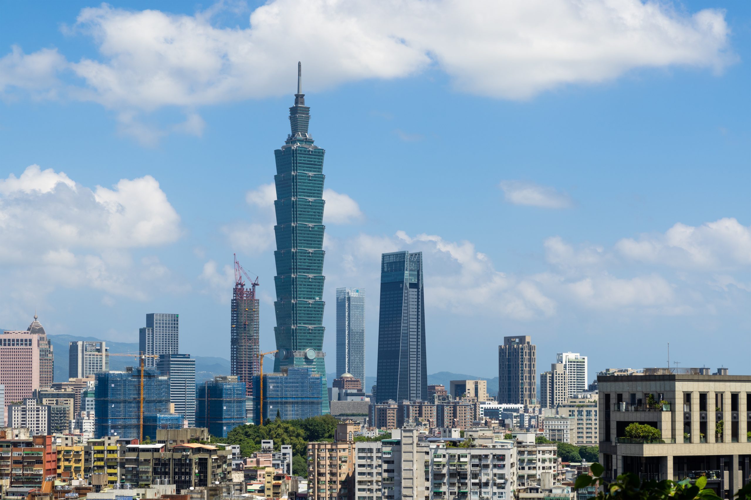
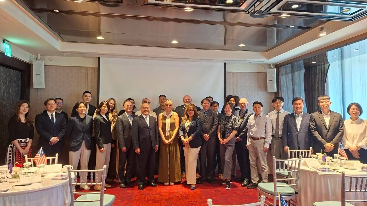
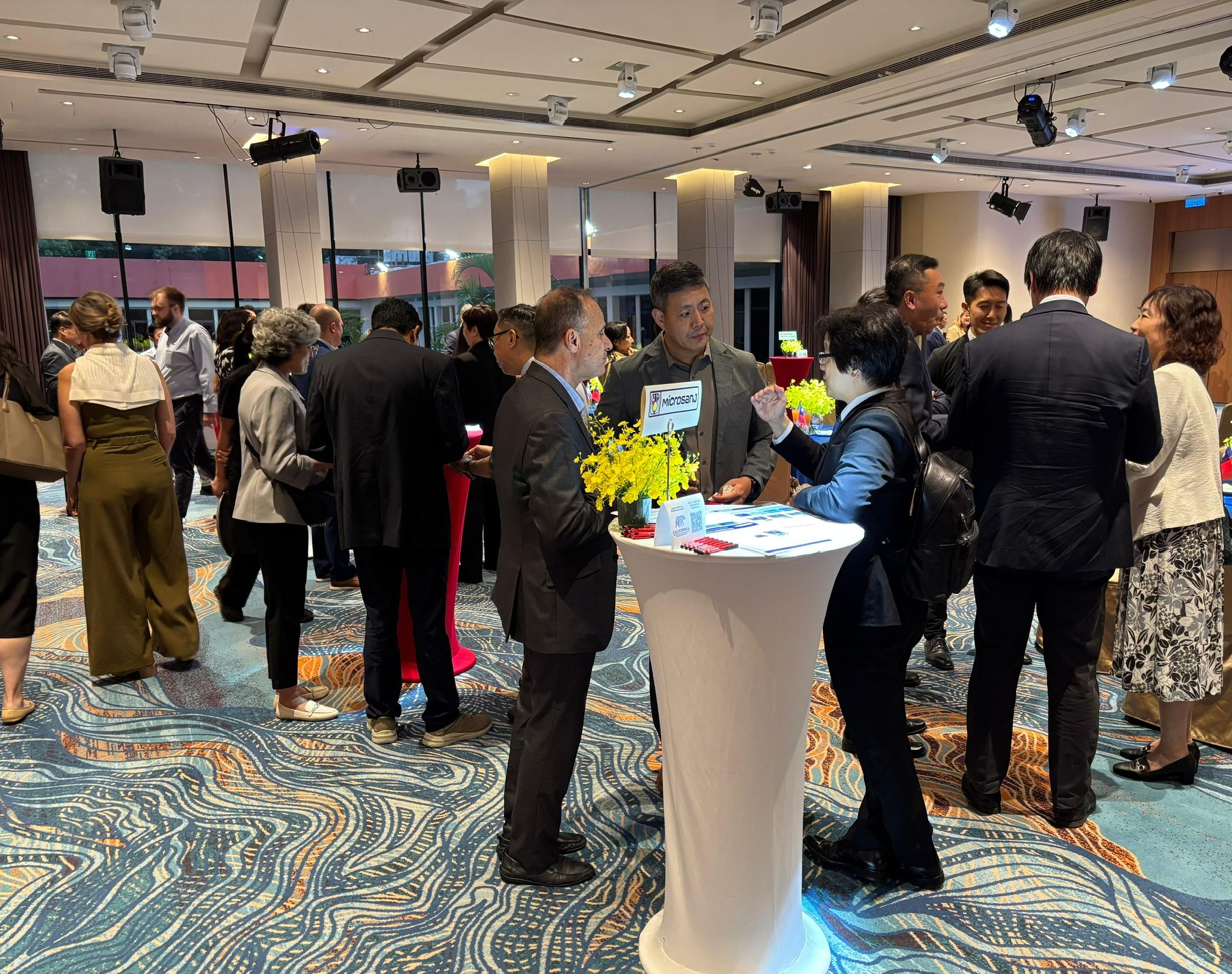
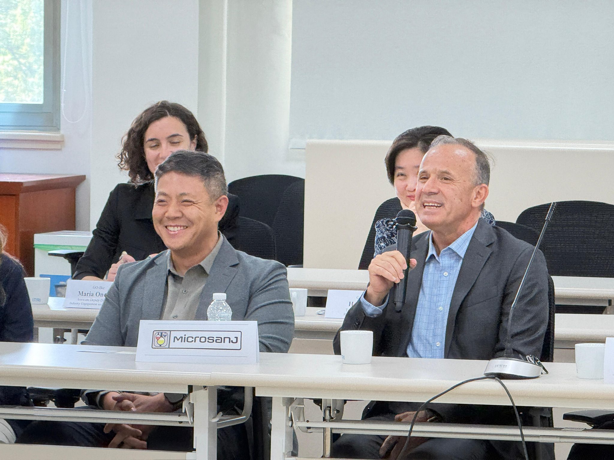
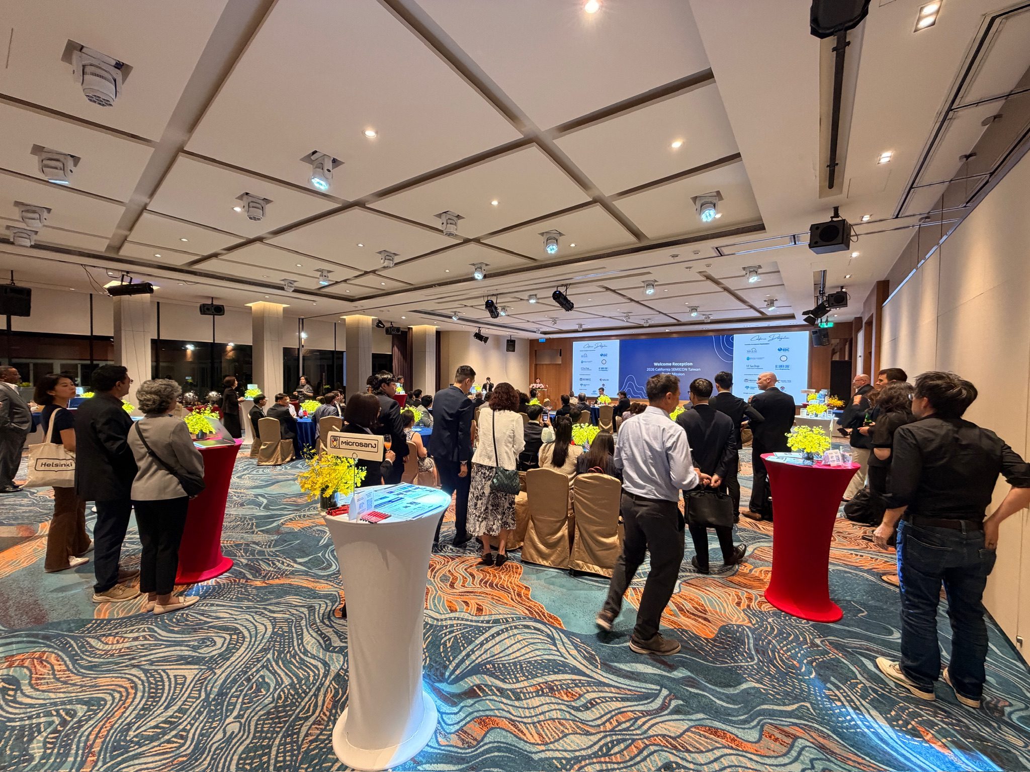
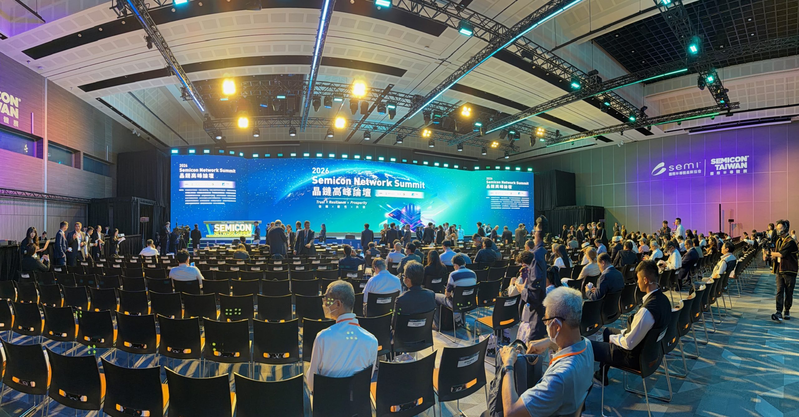
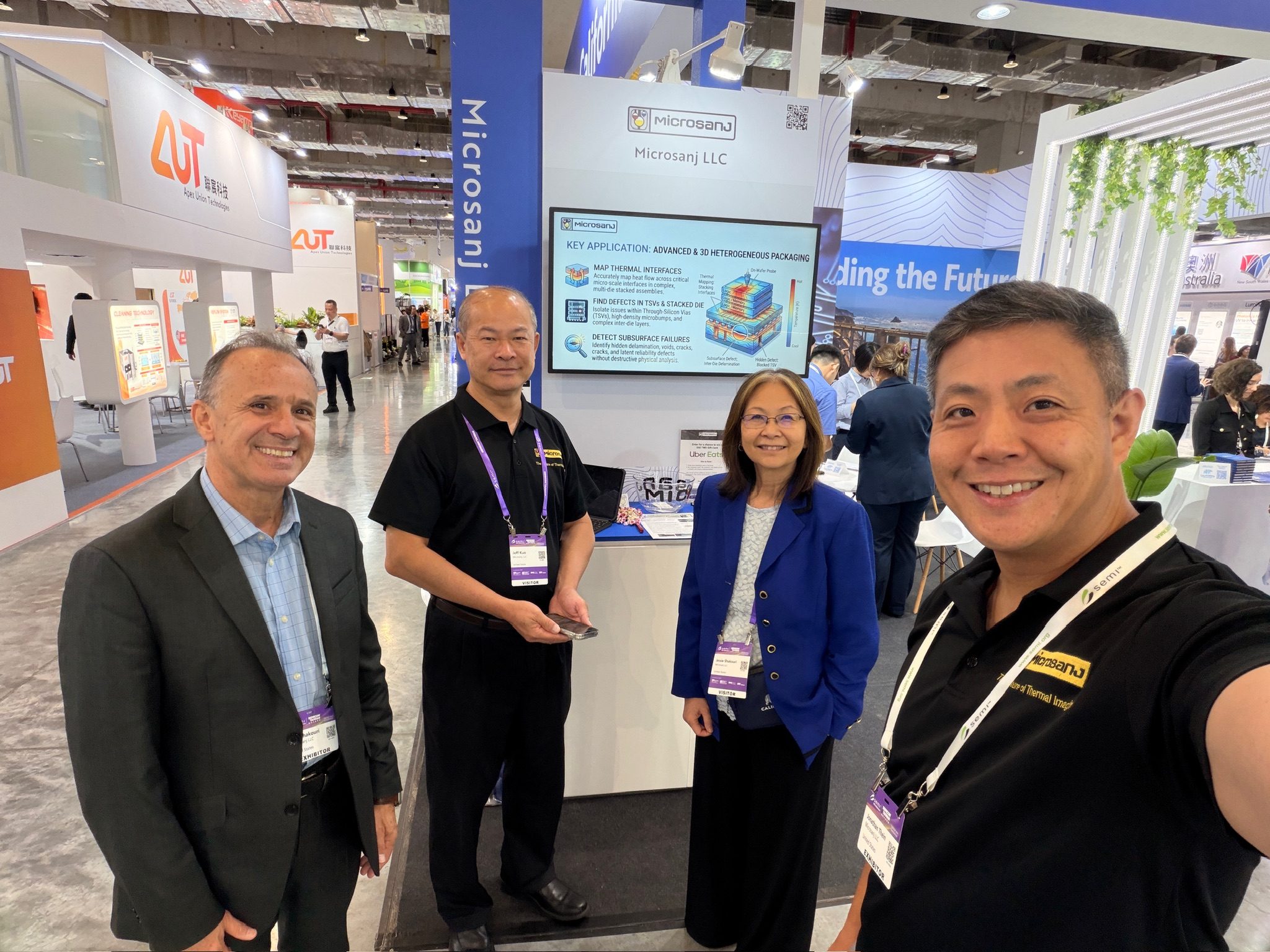
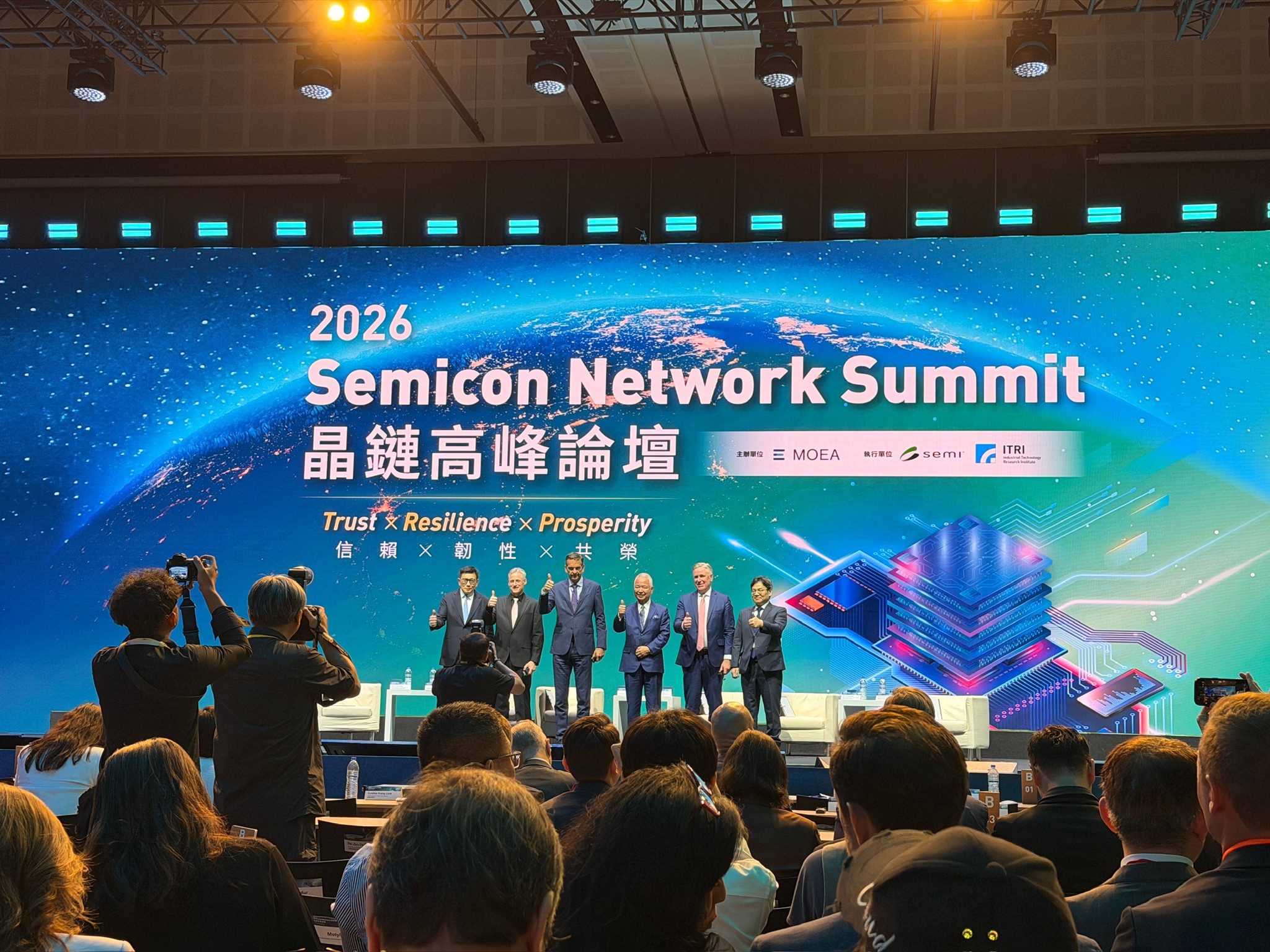
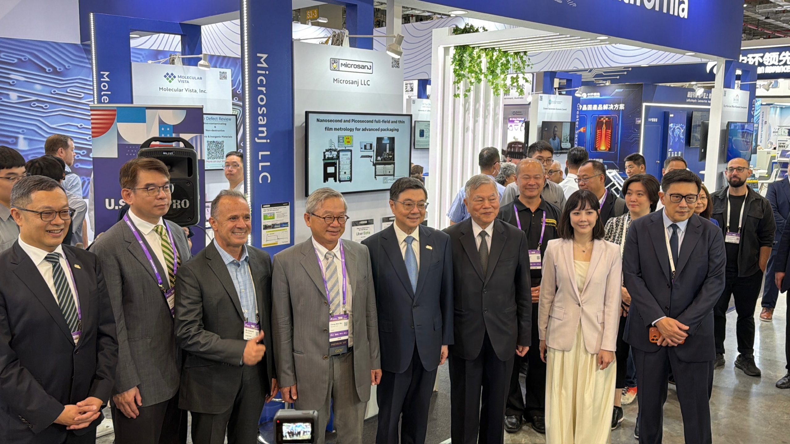
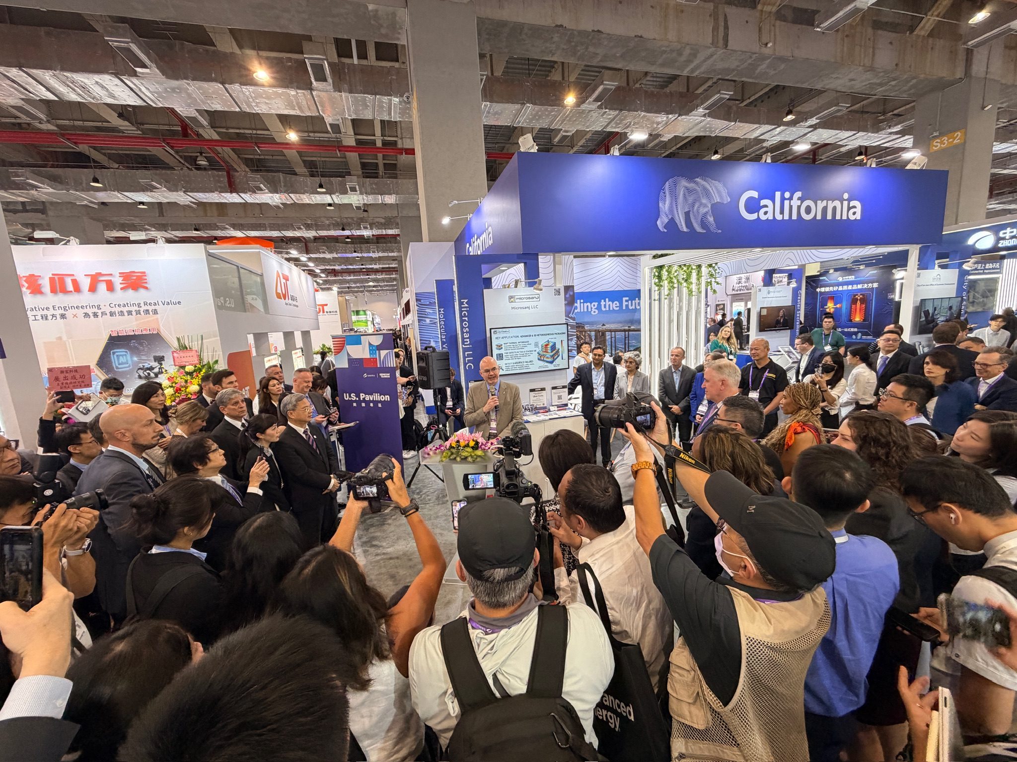
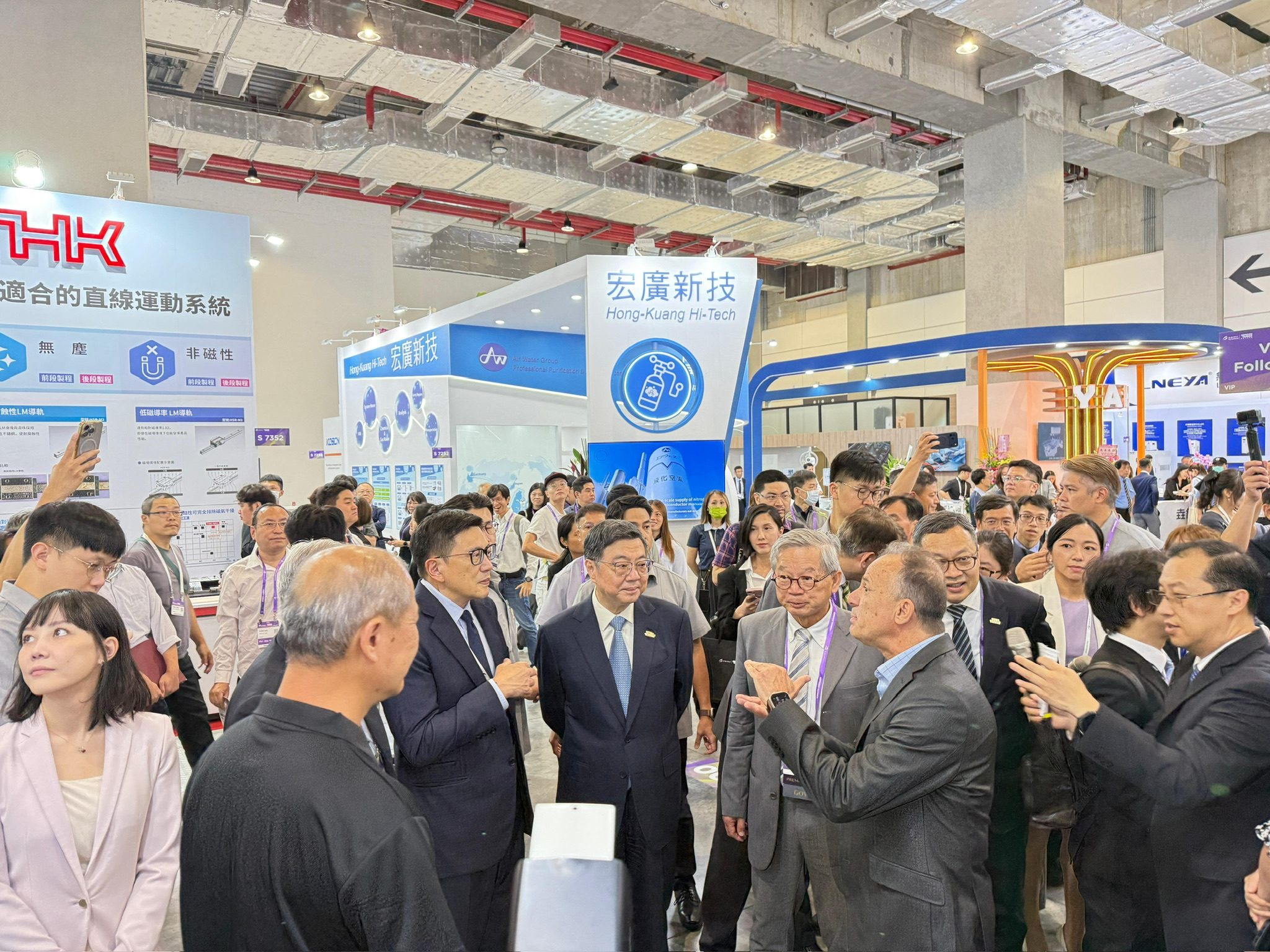
I just got back from a week in Taiwan as part of a California delegation organized through the state’s GO-Biz economic development program. We met with the institutions at the center of the semiconductor world — ITRI, Taiwan’s Ministry of Economic Affairs (MOEA), AmCham Taiwan — and had a surprise meeting with Taiwan’s Premier, Cho Jung-tai, and leadership from the American Institute in Taiwan (AIT). We were also on the ground for SEMICON Taiwan, which put the same conversation in front of foundries and OSATs on the show floor.
Different rooms, different audiences, but one question kept coming up in some form: how do we keep these devices from cooking themselves?
The Industry’s Center of Gravity Is Moving
For most of my career, the semiconductor roadmap was a wafer story: process nodes, transistor density, lithography. That story isn’t finished, but it’s no longer where the hardest engineering problems live. The action has moved downstream, to the package.
That was the throughline across every meeting, from research institutes to industrial policy to the show floor: packaging is now as strategically important as fabrication. The conversation has shifted from “how do we make more chips” to “how do we make chips into functioning systems without them overheating.”
That shift is what I want to spend the rest of this post on, because it’s the part of the story that doesn’t get enough attention: thermal management has quietly moved from an afterthought to a first-order design constraint.
What We Actually Talked About: Seeing Inside the Stack
Across nearly every meeting — including with AIT leadership, who wanted to understand what “made in California” deep tech looks like in this space — the conversation moved past thermal imaging in the general sense and into something more specific: how do you actually understand what’s happening inside a packaged, multi-layer device, layer by layer, interface by interface?
That’s a harder question than “where is the device hot.” A modern package isn’t one material — it’s a stack of dissimilar materials (GaN, SiC, Ga₂O₃, diamond, silicon, oxides, metals) bonded or interconnected through TSVs, interposers, and increasingly hybrid-bonded interfaces. Each junction has its own thermal boundary resistance (TBR), and TBR is frequently where a design’s thermal problems actually live — not in the bulk material, but in a thin, easy-to-overlook interface between two layers.
That’s the structure our NOSH-TDTR platform was built to characterize: in-plane and cross-plane thermal conductivity at each layer, TBR at specific bonded or TSV interfaces, and which material or junction in a complex stack is actually driving a bottleneck. It’s stack-level materials characterization on the real structure, not an idealized model of it — and as stacks get taller and more heterogeneous, knowing which specific layer or interface to fix is becoming part of how teams design the stack in the first place, not just how they validate it afterward.
Why the Device Stack Itself Is the Problem
It helps to think of this the way you’d think about buildings. A single-story house is a simple thermal problem: one structure, one roof, one set of walls, heat has nowhere complicated to go, and you can generally tell what’s wrong by looking at it from the outside. A high-rise apartment building is a completely different problem. Dozens of units are stacked on top of each other, each with its own systems, sharing walls, floors, and utility risers that carry heat, water, and power between units that were never designed to interact directly. You can’t manage a high-rise’s thermal comfort by inspecting it from the street — you need to know what’s happening floor by floor, wall by wall, riser by riser.
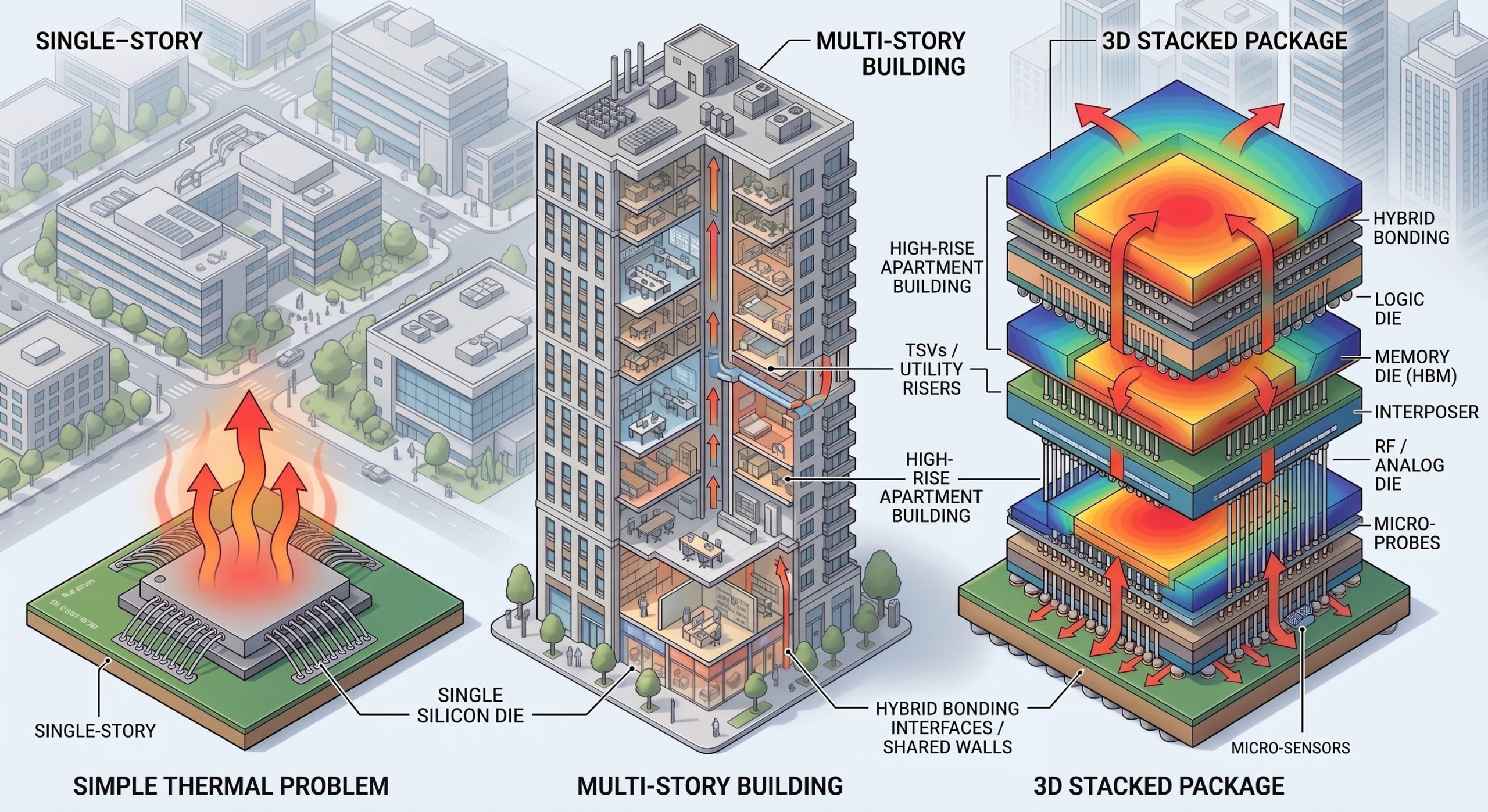
That’s effectively what’s happened to the chip package. The industry has moved from single-story construction to high-rise construction, and three things are converging to make that shift harder to manage:
3D heterogeneous integration (3DHI)
We’re no longer packaging a single function per die — we’re stacking logic, memory, RF, and sometimes multiple process nodes into one structure, the way a mixed-use tower stacks retail, offices, and apartments. Every interface between those “floors” is a potential place for heat to get trapped.
Hybrid bonding and TSVs
These interconnect approaches are replacing older methods and changing the thermal path in ways that aren’t always intuitive — the risers and shared walls of the structure. A stack that looks electrically sound can still have real TBR issues at the bonded interfaces — issues that only show up when you characterize the actual structure.
The move from single-layer to near-infinite stack
The industry’s appetite for “how much more can we stack” isn’t slowing down, and every additional layer adds another material transition and another place for heat to concentrate — another floor added to the building, with its own load on the systems below it.
Layered on top of that is a more literal shift in form factor: the move from circular wafers to square panels. A substrate that no longer has radial symmetry behaves differently, and the tools used to understand it have to adapt too.
Understanding all of this at the multi-layer, real-structure level isn’t optional anymore. It’s becoming a gating factor for how fast packaging innovation can move.
New Tools for a Different Kind of Building
A single-story house doesn’t need instrumentation to know something’s wrong — you can feel the draft or see the water stain. A high-rise does. And a high-rise built to run AI training clusters, quantum control electronics, and dense 3DHI stacks needs something else again: instrumentation built into the building itself, not just an inspector who visits after construction.
That was the other recurring theme in Taiwan: the tools the industry has relied on aren’t built for what AI, quantum, and 3DHI are now demanding of the package. Thermal characterization can’t stay a post-build validation step performed in a lab, on a sample, after the fact. It needs to move in two directions at once — earlier, into the design loop, so teams can predict where TBR will bite before a stack is ever fabricated; and later, into inline production, so interface issues get caught stack by stack, on the line, rather than discovered weeks afterward on a bench. AI workloads push power density higher, quantum devices push tolerances tighter, and 3DHI pushes structures taller and more heterogeneous — and each of those, in its own way, is asking for the same thing: a way to see inside the structure as it’s being built, not just after.
The Real Currency at an Event Like This: Trust
If there was one theme underneath every meeting, panel, and hallway conversation at SEMICON Taiwan, it was trust — not technology, not even capacity, but trust between the vendors, providers, and institutions that all have to work together to actually ship a packaged device.
That’s worth being specific about, because no single company sees the whole stack. The materials supplier doesn’t test the finished package. The OSAT doesn’t design the die. The tool provider doesn’t own the process recipe. When a thermal problem shows up, it shows up at an interface between two layers made by two different companies — and solving it requires those parties to share data and trust each other’s characterization enough to act on it together. That’s a genuinely hard problem in an industry built on IP protection and competitive advantage.
The ecosystem is working deliberately on exactly that. The best conversations we had on the show floor weren’t sales pitches — they were vendors and providers comparing notes candidly enough to figure out where the real gaps are. That’s the same spirit we try to bring to our own work: sharing clear, reproducible thermal data at the material and interface level, not just a black-box result. It’s how a foundry, an OSAT, and a materials supplier end up solving a stack-level thermal problem together instead of pointing at each other.
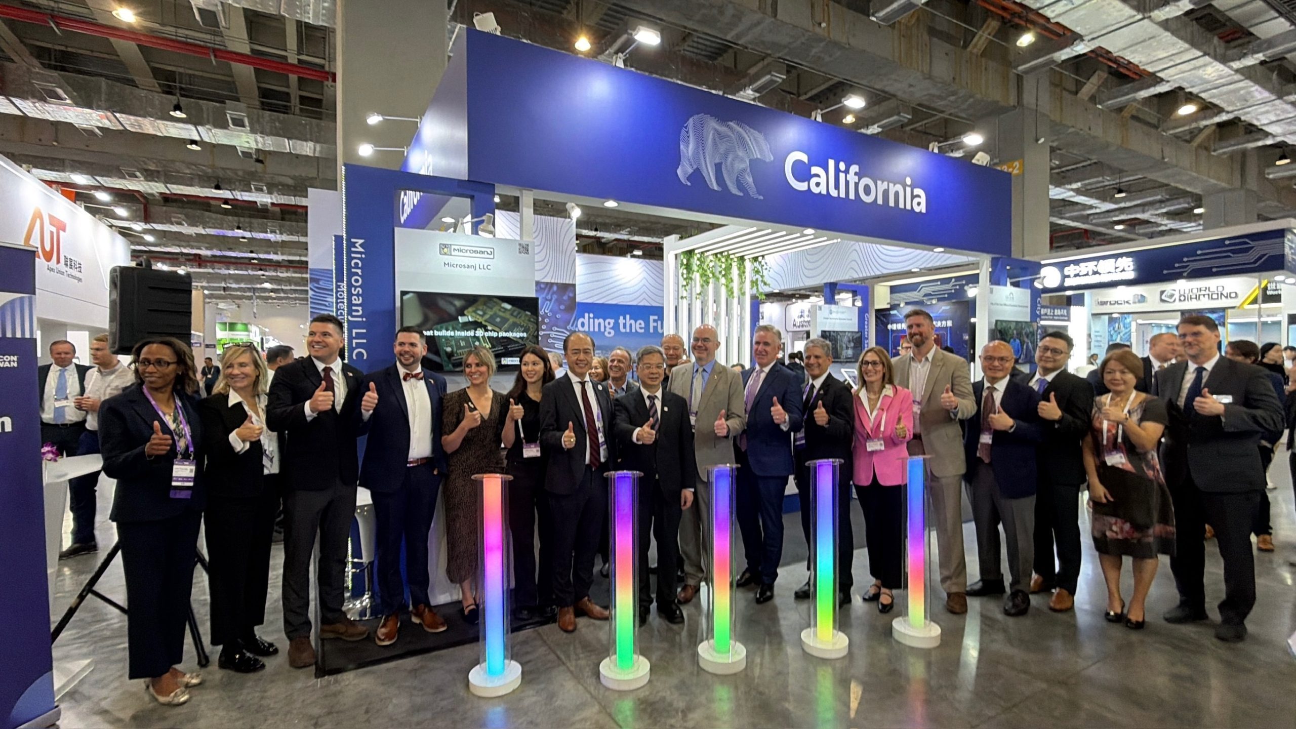
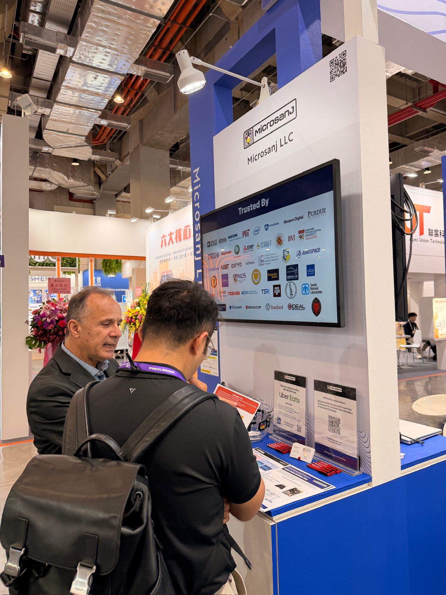
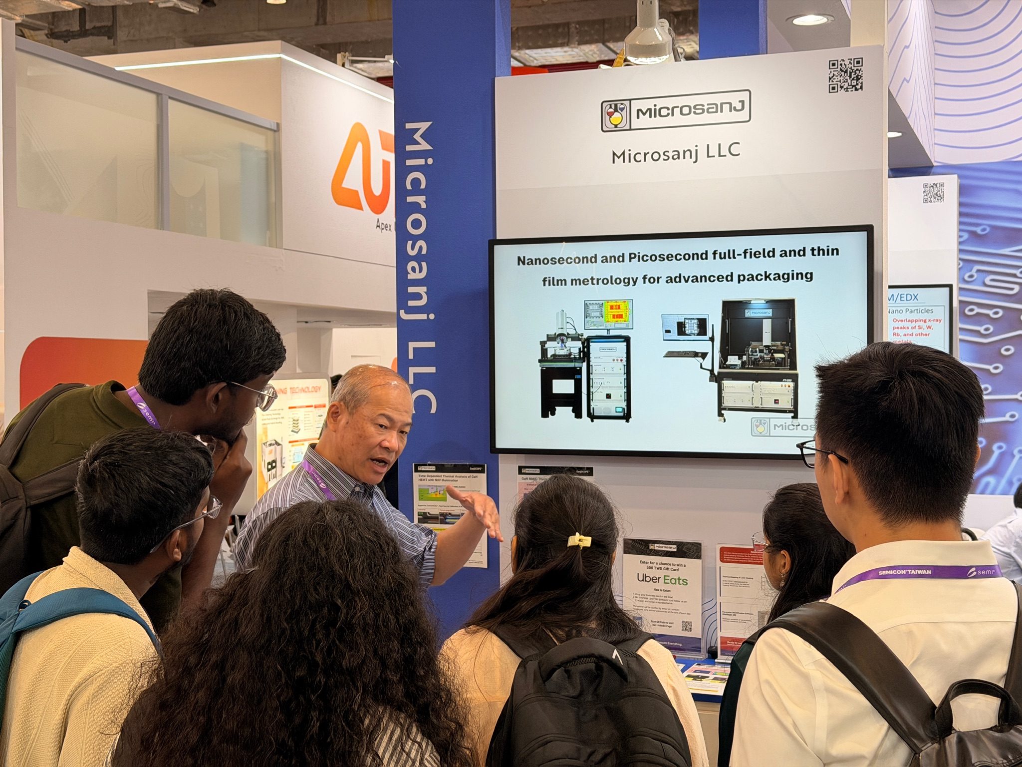
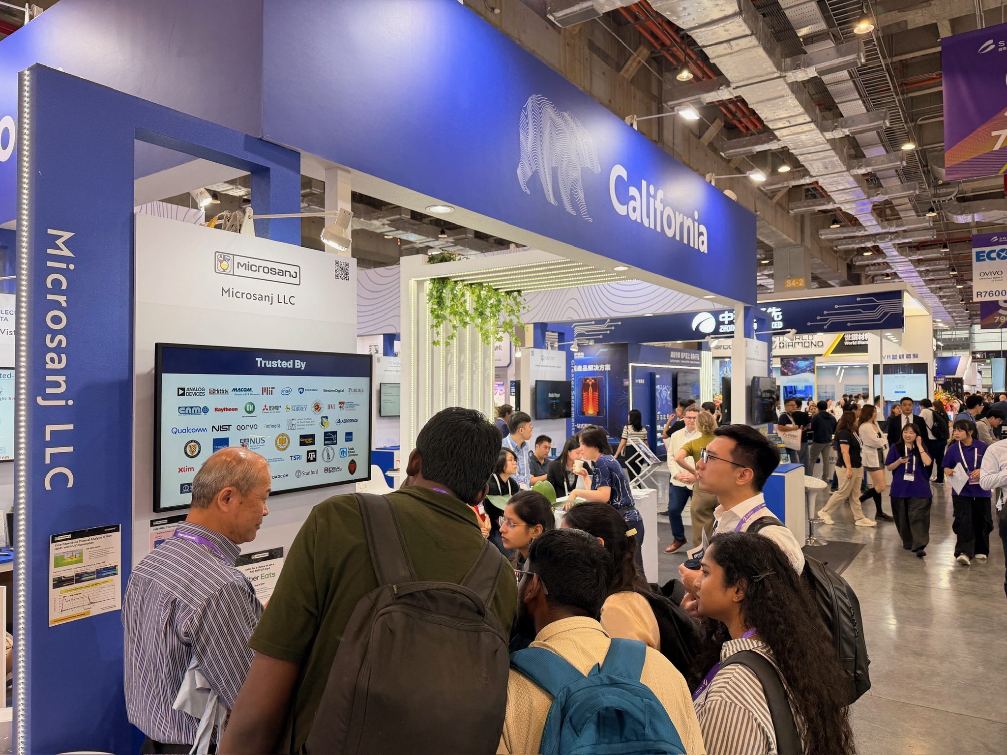
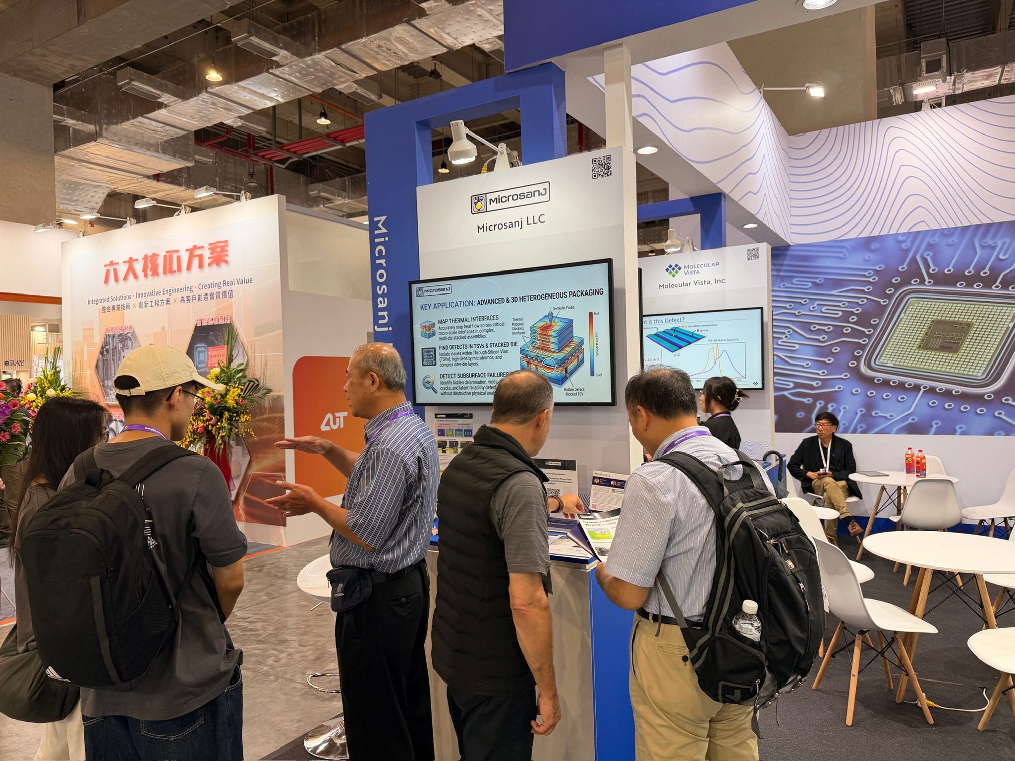
Thanks to GO-Biz for organizing the California delegation, to SEMICON Taiwan for hosting, and to the Anemone team for putting together a strong slate of meetings.
If you’re working through thermal challenges in advanced packaging and want to compare notes, I’d love to hear from you.